|
Main Product Parameters
|
|||
|
Growth method
|
Czochralski method
|
||
|
Crystal structure
|
M3
|
||
|
Unit cell constant
|
a=5.65754 Å
|
||
|
Density
|
5.323 g/cm3
|
||
|
Melt point
|
937.4 °C
|
||
|
Doped material
|
Undoped
|
Sb - doped
|
In / Ga - doped
|
|
Type
|
N
|
N
|
P
|
|
Resistivity
|
35 Ohm-cm
|
0.05 Ohm-cm
|
0.05~0.1 Ohm-cm
|
|
EPD
|
|
|
|
|
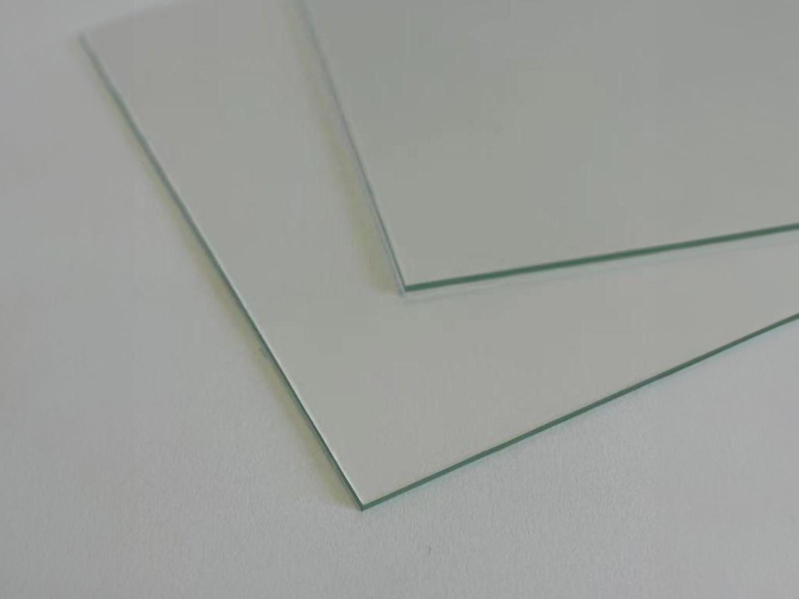
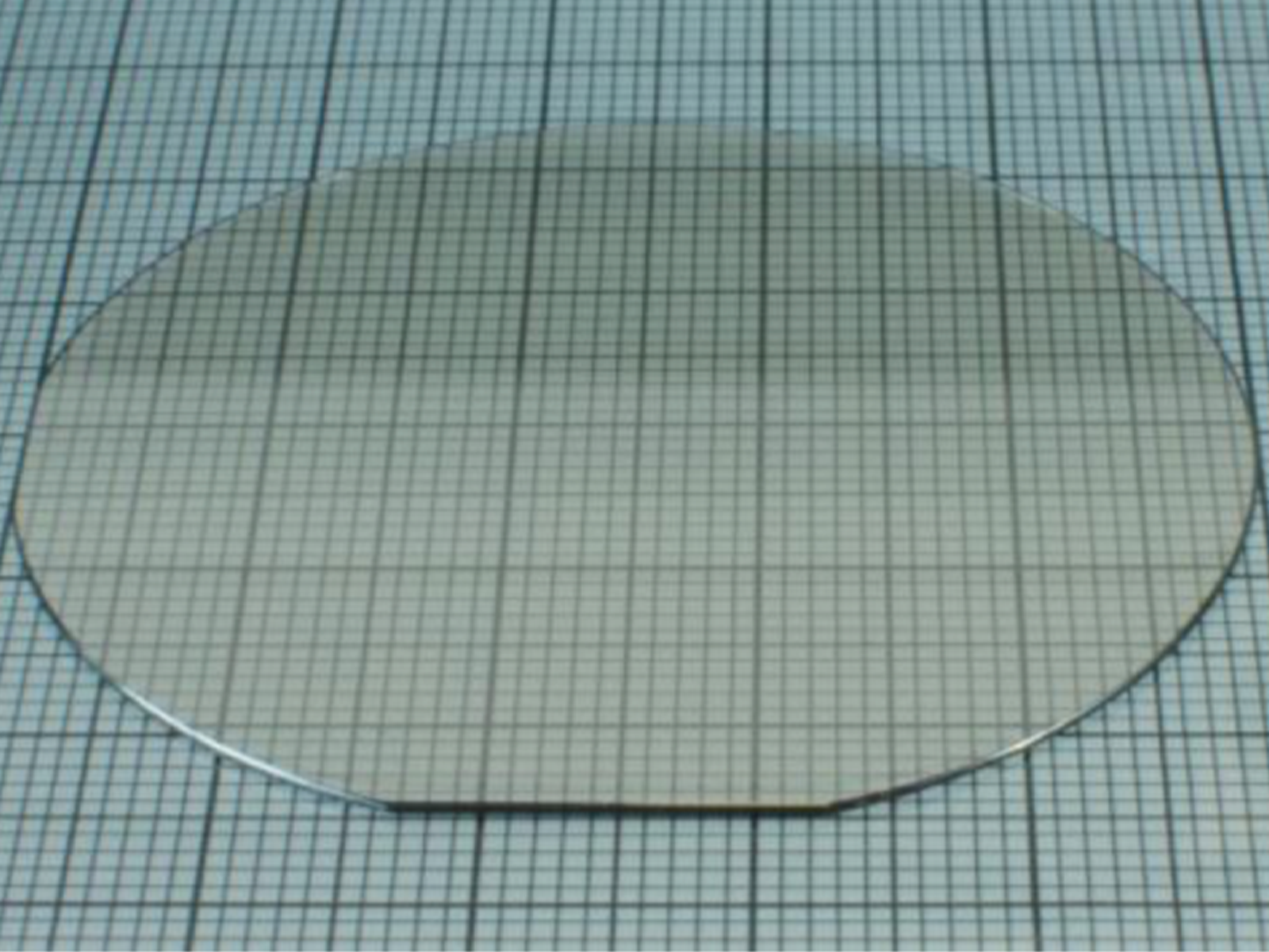
Size
|
10x5, 10x10, 15x15, 20x15, 20x20mm
|
||
|
dia 2" x 0.5mm, dia 1" x 0.5mm, other sizes are available upon request
|
|||
|
Thickness
|
0.5mm, 1.0mm
|
||
|
Polishing
|
Single or double side polished
|
||
|
Crystal orientation
|
(100), (110), (111)
|
||
|
Surface roughness Ra:
|
Rms or Ra ~ 5 A
|
||
|
Package
|
Sealed in class 100 clean bag packed in class 1000 clean room
|
||
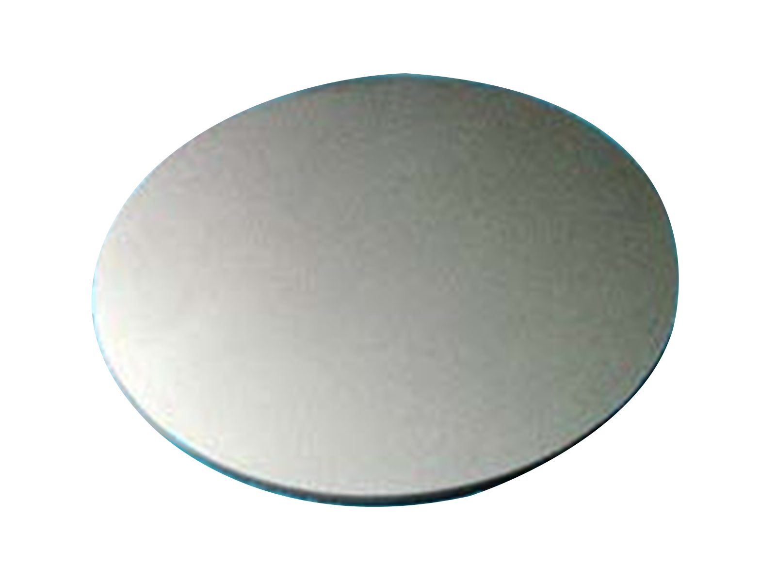
Ge Germanium Wafers and Crystal Substrates
SKU:
WA1420
SHIPPING:
Piece
IF YOU ARE INTERESTED IN A QUOTE FOR A LARGE QUANTITY, PLEASE CONTACT US
Email: Marknanossr@gmail.com
Email: Marknanossr@gmail.com
Ge Germanium Wafers and Crystal Substrates
| Piece | 1 |
Request a quotation.
Contact Us
Global Head Office
Email: Marknanossr@gmail.com
Tel:+86 15606950920
Wechat: 15606950920
Address: Building 1, No. 39 Xinchang Road, Haicang District, Xiamen City, Fujian Province, China
Contact Us
Global Head Office
Email: Marknanossr@gmail.com
Tel:+86 15606950920
Wechat: 15606950920
Address: Building 1, No. 39 Xinchang Road, Haicang District, Xiamen City, Fujian Province, China